
Hall Effect
- Page ID
- 315
\( \newcommand{\vecs}[1]{\overset { \scriptstyle \rightharpoonup} {\mathbf{#1}} } \)
\( \newcommand{\vecd}[1]{\overset{-\!-\!\rightharpoonup}{\vphantom{a}\smash {#1}}} \)
\( \newcommand{\dsum}{\displaystyle\sum\limits} \)
\( \newcommand{\dint}{\displaystyle\int\limits} \)
\( \newcommand{\dlim}{\displaystyle\lim\limits} \)
\( \newcommand{\id}{\mathrm{id}}\) \( \newcommand{\Span}{\mathrm{span}}\)
( \newcommand{\kernel}{\mathrm{null}\,}\) \( \newcommand{\range}{\mathrm{range}\,}\)
\( \newcommand{\RealPart}{\mathrm{Re}}\) \( \newcommand{\ImaginaryPart}{\mathrm{Im}}\)
\( \newcommand{\Argument}{\mathrm{Arg}}\) \( \newcommand{\norm}[1]{\| #1 \|}\)
\( \newcommand{\inner}[2]{\langle #1, #2 \rangle}\)
\( \newcommand{\Span}{\mathrm{span}}\)
\( \newcommand{\id}{\mathrm{id}}\)
\( \newcommand{\Span}{\mathrm{span}}\)
\( \newcommand{\kernel}{\mathrm{null}\,}\)
\( \newcommand{\range}{\mathrm{range}\,}\)
\( \newcommand{\RealPart}{\mathrm{Re}}\)
\( \newcommand{\ImaginaryPart}{\mathrm{Im}}\)
\( \newcommand{\Argument}{\mathrm{Arg}}\)
\( \newcommand{\norm}[1]{\| #1 \|}\)
\( \newcommand{\inner}[2]{\langle #1, #2 \rangle}\)
\( \newcommand{\Span}{\mathrm{span}}\) \( \newcommand{\AA}{\unicode[.8,0]{x212B}}\)
\( \newcommand{\vectorA}[1]{\vec{#1}} % arrow\)
\( \newcommand{\vectorAt}[1]{\vec{\text{#1}}} % arrow\)
\( \newcommand{\vectorB}[1]{\overset { \scriptstyle \rightharpoonup} {\mathbf{#1}} } \)
\( \newcommand{\vectorC}[1]{\textbf{#1}} \)
\( \newcommand{\vectorD}[1]{\overrightarrow{#1}} \)
\( \newcommand{\vectorDt}[1]{\overrightarrow{\text{#1}}} \)
\( \newcommand{\vectE}[1]{\overset{-\!-\!\rightharpoonup}{\vphantom{a}\smash{\mathbf {#1}}}} \)
\( \newcommand{\vecs}[1]{\overset { \scriptstyle \rightharpoonup} {\mathbf{#1}} } \)
\(\newcommand{\longvect}{\overrightarrow}\)
\( \newcommand{\vecd}[1]{\overset{-\!-\!\rightharpoonup}{\vphantom{a}\smash {#1}}} \)
\(\newcommand{\avec}{\mathbf a}\) \(\newcommand{\bvec}{\mathbf b}\) \(\newcommand{\cvec}{\mathbf c}\) \(\newcommand{\dvec}{\mathbf d}\) \(\newcommand{\dtil}{\widetilde{\mathbf d}}\) \(\newcommand{\evec}{\mathbf e}\) \(\newcommand{\fvec}{\mathbf f}\) \(\newcommand{\nvec}{\mathbf n}\) \(\newcommand{\pvec}{\mathbf p}\) \(\newcommand{\qvec}{\mathbf q}\) \(\newcommand{\svec}{\mathbf s}\) \(\newcommand{\tvec}{\mathbf t}\) \(\newcommand{\uvec}{\mathbf u}\) \(\newcommand{\vvec}{\mathbf v}\) \(\newcommand{\wvec}{\mathbf w}\) \(\newcommand{\xvec}{\mathbf x}\) \(\newcommand{\yvec}{\mathbf y}\) \(\newcommand{\zvec}{\mathbf z}\) \(\newcommand{\rvec}{\mathbf r}\) \(\newcommand{\mvec}{\mathbf m}\) \(\newcommand{\zerovec}{\mathbf 0}\) \(\newcommand{\onevec}{\mathbf 1}\) \(\newcommand{\real}{\mathbb R}\) \(\newcommand{\twovec}[2]{\left[\begin{array}{r}#1 \\ #2 \end{array}\right]}\) \(\newcommand{\ctwovec}[2]{\left[\begin{array}{c}#1 \\ #2 \end{array}\right]}\) \(\newcommand{\threevec}[3]{\left[\begin{array}{r}#1 \\ #2 \\ #3 \end{array}\right]}\) \(\newcommand{\cthreevec}[3]{\left[\begin{array}{c}#1 \\ #2 \\ #3 \end{array}\right]}\) \(\newcommand{\fourvec}[4]{\left[\begin{array}{r}#1 \\ #2 \\ #3 \\ #4 \end{array}\right]}\) \(\newcommand{\cfourvec}[4]{\left[\begin{array}{c}#1 \\ #2 \\ #3 \\ #4 \end{array}\right]}\) \(\newcommand{\fivevec}[5]{\left[\begin{array}{r}#1 \\ #2 \\ #3 \\ #4 \\ #5 \\ \end{array}\right]}\) \(\newcommand{\cfivevec}[5]{\left[\begin{array}{c}#1 \\ #2 \\ #3 \\ #4 \\ #5 \\ \end{array}\right]}\) \(\newcommand{\mattwo}[4]{\left[\begin{array}{rr}#1 \amp #2 \\ #3 \amp #4 \\ \end{array}\right]}\) \(\newcommand{\laspan}[1]{\text{Span}\{#1\}}\) \(\newcommand{\bcal}{\cal B}\) \(\newcommand{\ccal}{\cal C}\) \(\newcommand{\scal}{\cal S}\) \(\newcommand{\wcal}{\cal W}\) \(\newcommand{\ecal}{\cal E}\) \(\newcommand{\coords}[2]{\left\{#1\right\}_{#2}}\) \(\newcommand{\gray}[1]{\color{gray}{#1}}\) \(\newcommand{\lgray}[1]{\color{lightgray}{#1}}\) \(\newcommand{\rank}{\operatorname{rank}}\) \(\newcommand{\row}{\text{Row}}\) \(\newcommand{\col}{\text{Col}}\) \(\renewcommand{\row}{\text{Row}}\) \(\newcommand{\nul}{\text{Nul}}\) \(\newcommand{\var}{\text{Var}}\) \(\newcommand{\corr}{\text{corr}}\) \(\newcommand{\len}[1]{\left|#1\right|}\) \(\newcommand{\bbar}{\overline{\bvec}}\) \(\newcommand{\bhat}{\widehat{\bvec}}\) \(\newcommand{\bperp}{\bvec^\perp}\) \(\newcommand{\xhat}{\widehat{\xvec}}\) \(\newcommand{\vhat}{\widehat{\vvec}}\) \(\newcommand{\uhat}{\widehat{\uvec}}\) \(\newcommand{\what}{\widehat{\wvec}}\) \(\newcommand{\Sighat}{\widehat{\Sigma}}\) \(\newcommand{\lt}{<}\) \(\newcommand{\gt}{>}\) \(\newcommand{\amp}{&}\) \(\definecolor{fillinmathshade}{gray}{0.9}\)Hall Effect, deflection of conduction carriers by an external magnetic field, was discovered in 1879 by Edwin Hall. It has been known that moving carriers in a magnetic field are accelerated by the Lorentz Force, and the magnitude and the direction of the applied force on the carriers are given as in Equation (1):
\[ \mathbf{F} = q\boldsymbol{v}\times \mathbf{B} \label{1}\]
Where \(q\) is electron charge, \(\mathbf{v}\) is drift velocity and \(\mathbf{B}\) is magnetic flux density. If \(\mathbf{B}\) is perpendicular to current flow direction as seen in Figure \(\PageIndex{1}\), then the direction of the force is found by right hand rule and magnitude is expressed as scalar multiplication of \(q\), \(v\) and \(B\).
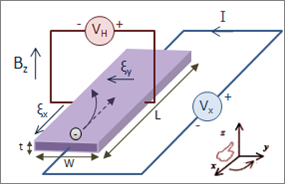
Figure \(\PageIndex{1}\) shows a conductive slab with a current \(I_x\) in x-direction, and with width \(w\) and thickness \(t\). An external magnetic flux density (\(B_z\)) is applied in z direction, resulting a Lorentz force in –y direction for holes and electrons (due to negative charge of electrons). Material shown in Figure \(\PageIndex{1}\) is a p-type semiconductor (doped with acceptor atoms). Without application of any magnetic field, holes flow through by experiencing no force along the y-direction. However, once \(B\) is applied, holes are deflected in –y direction resulting a (+) charge accumulation on the side A. Since the material has to be neutral, same amount of charge with opposite sign (-) appears on the other side of the slab (side \(B\)). Source of this negative charge on side B is negatively charged dopant ions. An internal electrical field (\(\varepsilon_y\)) starts building. As more charge accumulates on the sides, (\varepsilon_y\) gets stronger and opposes the Lorentz force. Eventually, electrical force (\(F_y=q\varepsilon_y\)) cancels out the Lorentz force (\(-qvB_z\)) and results:
\[ \varepsilon_{y} = v B_{z} \label{2}\]
Also, current density (\(J_x\)) and the drift velocity (\(v\)) are also related with:
\[ J_{x} = pqv \label{3}\]
Where p is the hole density of the material. When \(v\) in (3) is substituted in (2):
\[ \varepsilon _{y} = \dfrac{J_{x}B_{z}}{pq} \label{4}\]
is achieved. Also, voltage potential difference between \(A\) and \(B\) (\(V_{AB}\)) can be written as:
\[ V_{AB} = \dfrac{R_{H}I_{x}B_{z}}{t} \label{5}\]
Where \(R_H\)(=1/qp)is Hall coefficient. In (5), all parameters except \(R_H\) are known or can be measured, which gives solution to \(R_H\), so p. If a similar derivation is performed for an n-type material (majority carriers are electrons), \(R_H= -1/ qn\) will be achieved. Since \(R_H\) is found to be positive for p-type material and negative for the n-type, Hall coefficient can be measured to analyze the type of majority carrier of an unknown material.
Furthermore, if the resistivity (\(\rho\)) of the material is known (or measured) mobility of the carriers can also be extracted as given:
\[ \mu_{h}=\dfrac{\sigma }{qp}=\dfrac{R_{h}}{\rho } \label{6}\]
Where \(\mu_p\) is hole mobility. Relation in (6) enables mobility measurements of majority carriers for single carrier materials.
Cannot fetch Flickr photo (id: 3356444015). The photo either does not exist, or is private
Figure \(\PageIndex{2}\) Hall effect in presence of both holes (h) and electrons (e) \(^{[3]}\).
If both holes and electrons are conduction carriers, then a different derivation has to be done to solve for Hall coefficient. Figure \(\PageIndex{2}\) shows a semiconductor with holes and electrons flowing through. Magnetic flux density B deflects both carrier types to bottom surface of the material. In this case, Lorentz force on electrons and holes can be written as:
\[ F_{e}=qv_{e}B \label{7}\]
\[ F_{h}=qv_{h}B \label{8}\]
\[ \varepsilon_{e}=\dfrac{J_{e}B}{qn} \label{9}\]
\[ \varepsilon_{h}=\dfrac{J_{h}B}{qp} \label{10}\]
In transient analysis, current density along y-axis (perpendicular to electrical current flow) can be written using (9) and (10):
\[ J_{y}=nq\mu_{e}\varepsilon_{e} + pq\mu_{h}\varepsilon_{h}+ (nq\mu_{e} + pq\mu_{h})\varepsilon_{H} \label{11}\]
In steady state, current density (net charge flow) along the y-axis has to be zero, which results in Hall coefficient of:
\[ R_{H}=\dfrac{p\mu_{h}^{2}-n\mu_{e}^{2} }{q(p\mu_{h}+n\mu_{e})^{2}} \label{12}\]
Equation (12) indicates that Hall coefficient of a material can either be positive or negative depending on mobility and density of the carriers (electrons and holes). Table \(\PageIndex{1}\) shows Hall coefficient of a number of metals. Notice that \(R_H\) is positive for some metals, showing holes are the dominant type.
| Li | Na | Cu | Ag | Au | Zn | Cd | Al |
|---|---|---|---|---|---|---|---|
| -1.7 | -2.5 | -0.55 | -0.84 | -0.72 | +0.3 | +0.6 | -0.3 |
References
- F. T. Ulaby, Electromagnetics for Engineers. ,4th ed.NJ: Pearson/Prentice Hall, 2005, pp. 397.
- B. G. Streetman, Solid State Electronic Devices. ,4th ed.Prentice Hall, 1995.
- M. A. Omar, Elementary Solid State Physics: Principles and Applications. MA: Addison Wesley Publishing Company, 1993, pp. 669.
Contributors and Attributions
ContribMSE5317